Unlocking the Potential of Gold Finger PCBs in Telecommunications
Table of contents:
Improving Data Transfer Speeds with Advanced PCB Gold Fingers
The Impact of Multilayer PCB Technology on Signal Integrity
Gold Finger PCB Solutions for Next-Generation Communication Systems
Enhancing Reliability in Telecom Hardware with Double Layer PCBs
Improving Data Transfer Speeds with Advanced PCB Gold Fingers
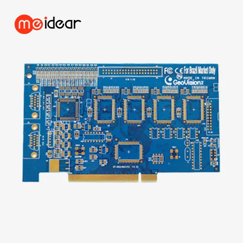
Gold Finger PCBs are making significant strides in improving data transfer speeds within telecommunications infrastructure. The precision-engineered gold-plated connectors ensure minimal signal loss and enhanced conductivity, crucial for high-speed data transmission. Multilayer PCB manufacturers have optimized these components to withstand the rigorous demands of modern telecom systems. By incorporating Gold Finger PCBs, network equipment can achieve faster and more reliable connections, essential for the ever-increasing data demands of 5G networks and beyond. The durability of gold-plated connectors also contributes to the longevity of telecom hardware, reducing maintenance needs and improving overall system reliability.
The Impact of Multilayer PCB Technology on Signal Integrity
Multilayer PCB technology has transformed the landscape of telecommunications hardware design. By leveraging multiple layers, PCB assembly solutions can now accommodate more complex circuits within a compact form factor. This advancement is particularly beneficial for signal integrity in high-frequency applications. Multilayer PCB manufacturers have perfected techniques to minimize electromagnetic interference between layers, resulting in cleaner signal transmission. The integration of Gold Finger PCBs with multilayer designs further enhances this capability, offering unparalleled performance in signal quality and consistency. This synergy between multilayer technology and gold-plated connectors is pushing the boundaries of what's possible in telecom equipment design.
Gold Finger PCB Solutions for Next-Generation Communication Systems
As we move towards next-generation communication systems, Gold Finger PCBs are playing a pivotal role in meeting the escalating demands of the industry. PCB assembly services are adapting to incorporate these advanced components into cutting-edge designs for 5G and future 6G networks. The superior connectivity and durability of Gold Finger PCBs make them ideal for the high-frequency, high-bandwidth requirements of modern telecom infrastructure. Multilayer PCB manufacturers are continuously innovating to create PCB assembly solutions that can handle the increased complexity and performance needs of these systems. By leveraging Gold Finger PCB technology, telecom companies can build more robust, efficient, and future-proof networks. This advanced technology ensures stronger connections, improved durability, and enhanced signal transmission, making it ideal for supporting high-performance telecom systems. With its reliability and scalability, Gold Finger PCB technology is a key component in meeting the growing demands of modern communication networks.
Enhancing Reliability in Telecom Hardware with Double Layer PCBs
Double Layer Gold Finger PCBs represent a significant leap forward in enhancing the reliability of telecom hardware. These specialized PCBs offer a perfect balance between complexity and performance, making them suitable for a wide range of telecom applications. PCB assembly services have embraced double layer designs as they provide ample space for intricate circuit layouts while maintaining excellent signal integrity. The gold-plated connectors on these PCBs ensure consistent performance even in challenging environmental conditions, a critical factor for outdoor telecom equipment. Multilayer PCB manufacturers have optimized the production process for these double layer boards, ensuring high quality and cost-effectiveness for telecom hardware manufacturers.
The integration of Gold Finger PCBs in telecommunications has ushered in a new era of performance and reliability. From enhancing data transfer speeds to improving signal integrity, these advanced PCBs are essential components in modern telecom infrastructure. Multilayer PCB manufacturers continue to push the boundaries of what's possible, developing innovative PCB assembly solutions that meet the evolving needs of the industry. As we look to the future of telecommunications, it's clear that Gold Finger PCBs will play a crucial role in shaping the next generation of communication systems, offering the durability, precision, and high-performance capabilities required for our increasingly connected world.


Comments
Post a Comment